|
The c300 up close
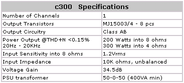
This 300 Watts/RMS amplifier is meant for
those who are not only looking for higher power, but
superior performance as well. In order to achieve
this, the c300 features some advanced techniques that
are absent in its' smaller counterpart (c200).
Additions
in 1st Gain Stage
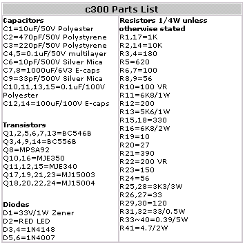
Cascodes
Right at the very first gain stage, cascodes
(Q5,6) are adopted. They serve to improve the high
frequency performance of the c300. These cascodes
are biased to approximately midpoint between 0V and
+V by zener diode D1 (33V).
Current
Mirrors
The first stage also contains current mirror
Q3,4. As the name implies, the mirror forces equal
current in the LTP (long tail pair). It is known for
its' active loading and high gain properties.
Emitter
Degeneration Resistors
Slew rate of the input differential is improved by
resistors R6,7,8,9,10. In the absence of matched transistors,
preset R10, is used for trimming DC to a minimum at
the output of the amplifier.
Buffering
the 2nd Stage
The
VAS mod
The 2nd stage is direct coupled to the differential
via a darlington Q8. This effectively buffers Q10,
the main transistor that is amplifying the voltage
from loading the preceding stage. Q10 is biased into
class A by constant current source Q12. Capacitor
C9 sets the dominant pole in Miller compensation.
Thermal
Tracking
The
remaining parts of the circuit is conventional. Vbe
multiplier Q11, adjust the bias for the output transistors
which is in full complementary EF configuration. Q11
must be thermally coupled to the main power heatsink
for proper thermal tracking. VI Limiting network consists
of Q13,14, R25~30 and D3,4. This network is optional,
and can be omitted if desired. |
THD of c300

Biasing
of output transistors
All THD readings were done with outputs biased to
20mV across 0.39 ohms emitter resistor. This works
out to approximately 55mA per output transistor in
idling state.
1
| 2 | 3
| 4 | 5
| 6 | 7
| 8
Download
c300 High Res Schematics |
